IISc-WORKFLOW-SMARTPHONE-VLC_Transmitter
JUST A WEBSITE DETAILING MY Research-Project in IISc.
REPO_LINK! . [!! CONFIDENTIAL please reach out to me at vv50517@gmail.com for any queries regarding this]
I welcome everyone to my webpage detailing my research-project in IISc. This project was a very challenging one but I had compressed my workflow to include important details and milestones. For in-detail reference to codes and other results, visit my repo_link above. I am also really thankful to Professor Chockalingam who gave me the support and platform to do this wonderful research-project.
Below is the Workflow!
A. Feb 11 : An Email from Prof Chockalingam citing the need for using smartphone’s flashlight as a transmitter of Information. He shared a paper to start with A study done by a chinese university . From then, i started to research and work on the same.
B. Came by Android studio as the best IDE for android app development as ease of loading the app into the smartphone. Started Developing the program and used the Camera Interface of the smartphone to access and control my flashlight.
C. Started developing the code , and used sleep function of thread as the function that implements the pulse width of my flashlight signal (either-on or off).
D. Built a simple reciever circuit consisting of a photodiode and lm358 op-amp , and Arduino Uno acting as the intelligence.
E. Flashed a simple clock signal consisting of 0s and 1s alternating for 100 times (hereby called the clock signal from now on) onto the reciver circuit, probed an oscilloscope to view the output. (Look at clock_inconsitency.docx document to view the problem in detail , i have attached the link below)
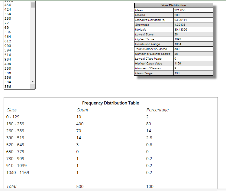
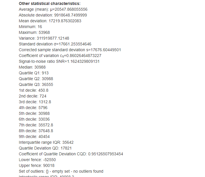
F. A major problem became existent, the pulse width is deviating from the programmed pulse width rapidly . I programmed a 1 ms pulse width and the output pulse width varied from 5 ms to 15 ms. Thus a deviation of 500 to 1700% from my programmed width is noted. A statistical test has been conducted to find the mean and variance of the pulse widths, the result is indicated in detail by
G. As an alternative way of programming the pulse width, i used java’s Executor Object to achieve my objective. It has a comparatively better performance in terms of less divergence of pulse width, the result is indicated in detail by
.PNG) .
.
But it is still not a solution , just an alternate way in which we faced the same problem .
H. The chinese paper also detailed the same problem, but their solution was not clearly stated in the paper, and we were left in a state of perusal on how to resolove the problem by ourselves.
I. Landed on a new study . They also detailed the same problem, and also had added that the pulse width variation varied for different smarphones as the problem is hugely OS dependent (OS introduces the delay as it is a GPOS and multithreaded). But they had proposed a solution to this problem. Encoding 1 and 0 in terms of pulse width was their attempt. I wrote a report that details how i collected the gist from several sources the HAL paper was one of them and had arrived at a solution CLOCK_INCONSISTENCY.DOCX
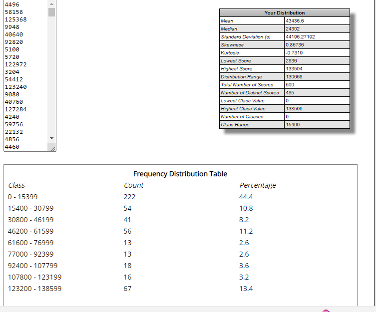
J. So i was able to arrive at a solution and was able to flash my information ( eg:”chockalingam” in string (utf-8 encoding)). But there was a huge take , the data rate was too low, it was around 17 bits/second ( hereforth called bps) , which is too low by any standard and a motivation to increase the data rate was existent. Also i subsequently measured other metrics like BER and Eb/No (Noise is modelled with Shot noise as the only one, thermal noise is ignored). Thus it has a BER 0.054 of and Eb/No of 40,469(no unit).(all metrics calculated by performing ST(see [1]))
K. In parallel, i also developed a fingerprint authentication feat to my modulation app to add additional security. The feat was achieved with the help of FingerprintManager module in android studio.
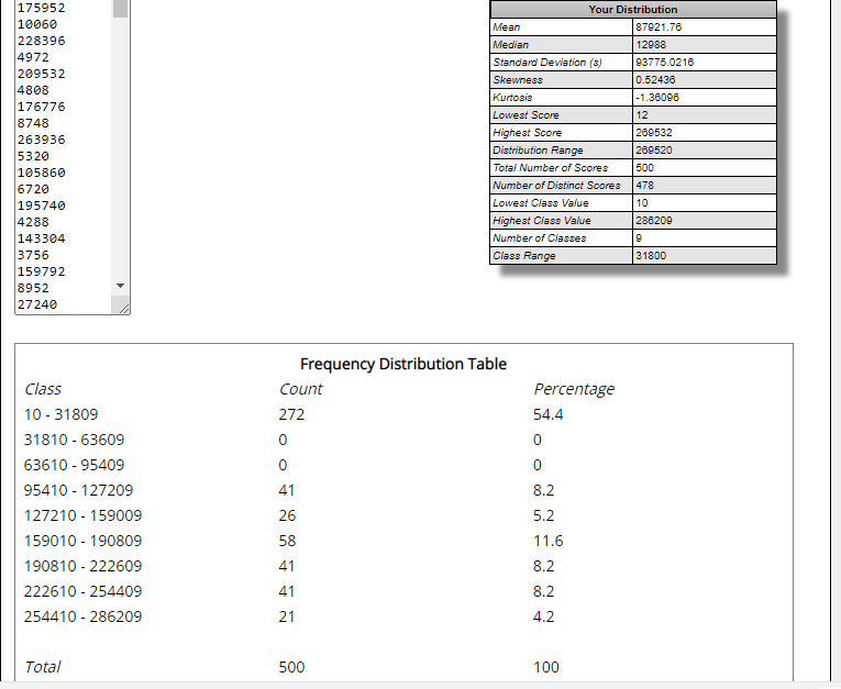
L. Subsequently i rethinked that any 2 consecutive bits should have should have their equivalent symbol high time to be seperated by 17ms and made 0’s symbol without any delay , whereas 1 symbol’s high time is programmed to be 17ms long . Even though the clock pulses varied even in this case , i was able to transmit and recieve the data properly and was able to increase my datarate to 54 bps , BER of 0.0125 and Eb/No of 48,787(ST).
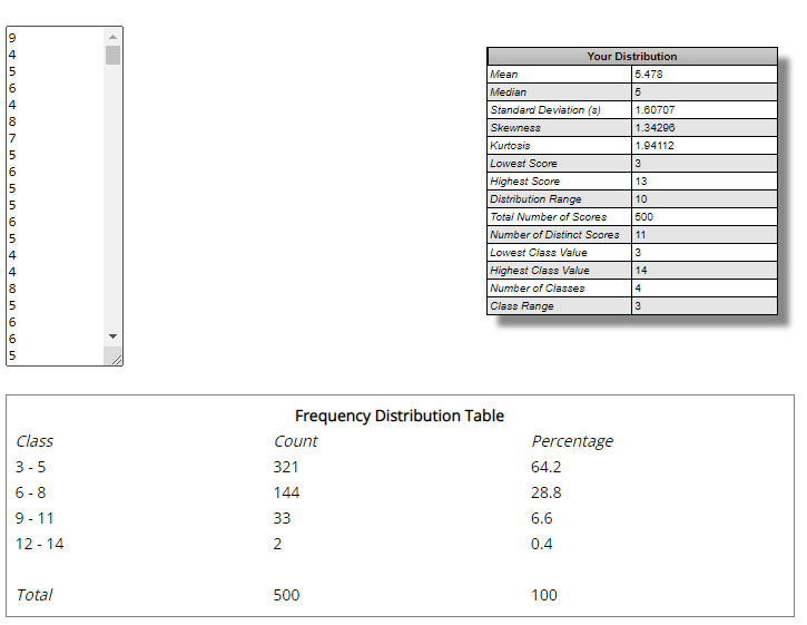
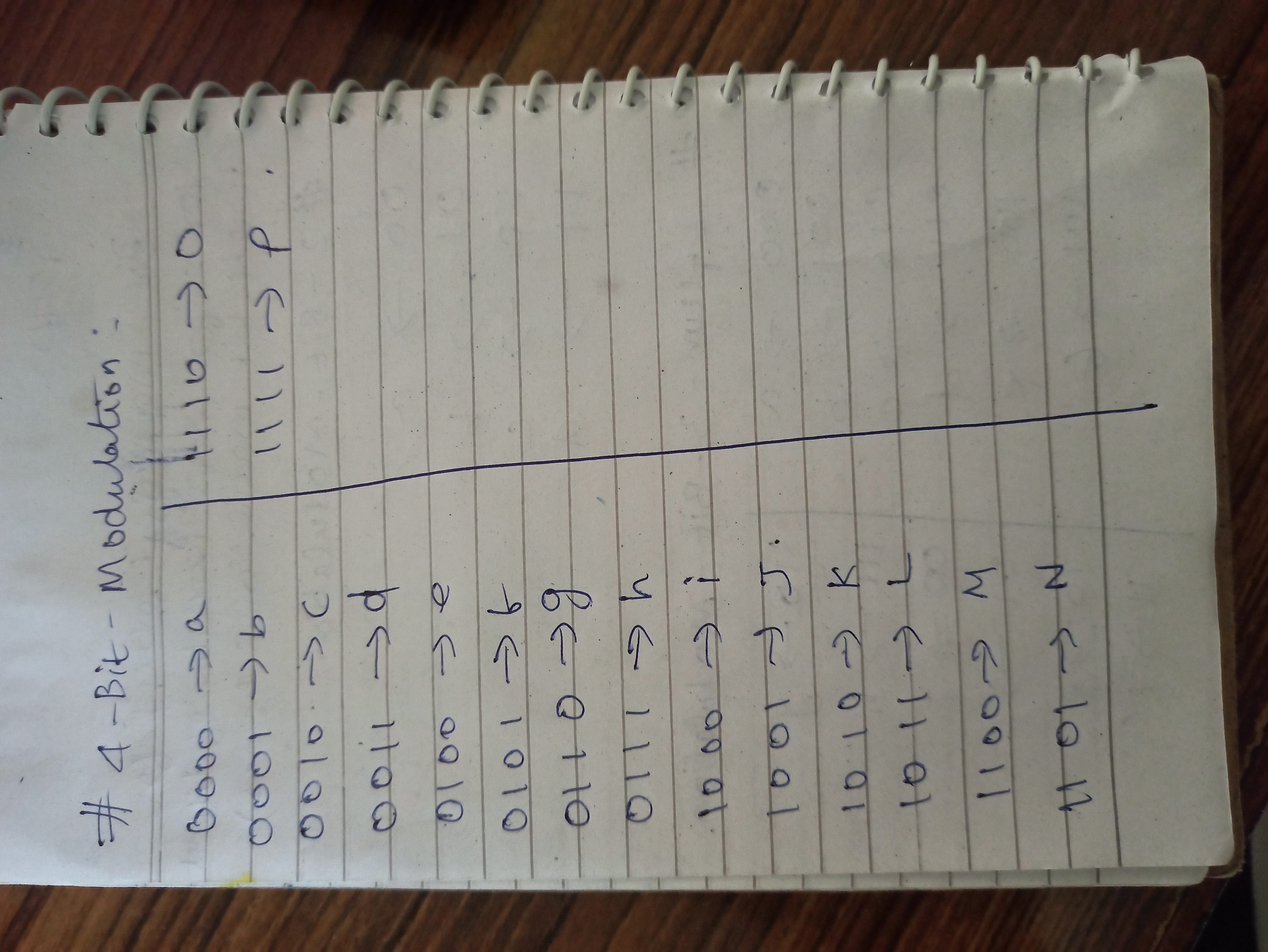
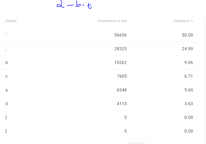
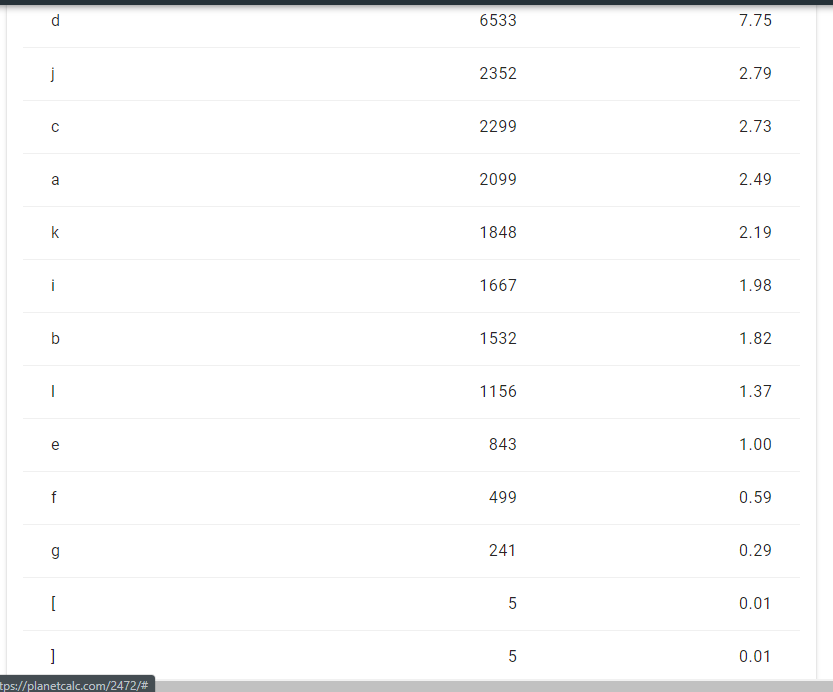
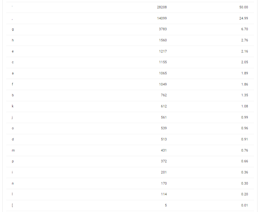
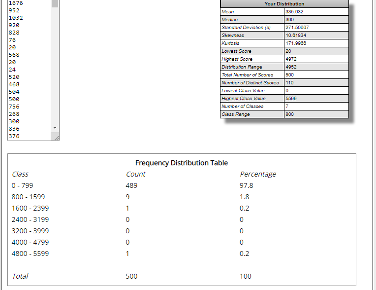
M. As a next step , i came to know of Source-Coding as a way of compressing the data and maximizing the data rate. In particular, i implemented Multi-Bit-Modulation as a solution. (One difference from normal source coding and my-kinda source coding is that, normally 0s and 1s are the final layer of abstraction in all coding stratergies, but in my kind, special symbols are the final one , because my source is itself inconsistant!). Firstly, i implemented 2-bit-modulation where 00,01,10 and 11 are allocated respective symbols which are seperated consecutively by 17ms (the threshold gap for Redmi-Note-5-Pro). The symbols are allocated based on the probability of occurence of bi-bits(a way that i use to call 2 bits). For a particular string found out that 01 and 10 are the first two most probable bi-bits, whereas 00 and 11 are the least probable bi-bits . Thus the symbol with less duration gets allocated to the most probable bi-bits. Thus i was able to increase my data rate ranging from 64 to 80 bps. But in these, i specifically modified the reciever code for each string. But this is not a realistic solution simply because there are literally infinite names and modifying reciever code for each one is not a viable solution. Thus i ran a research for 500 random strings and found out a clear biasness in data for 3 types of modulation that i had carried out. Before Looking at the Freq Distribution ,look at the mapping that i have used
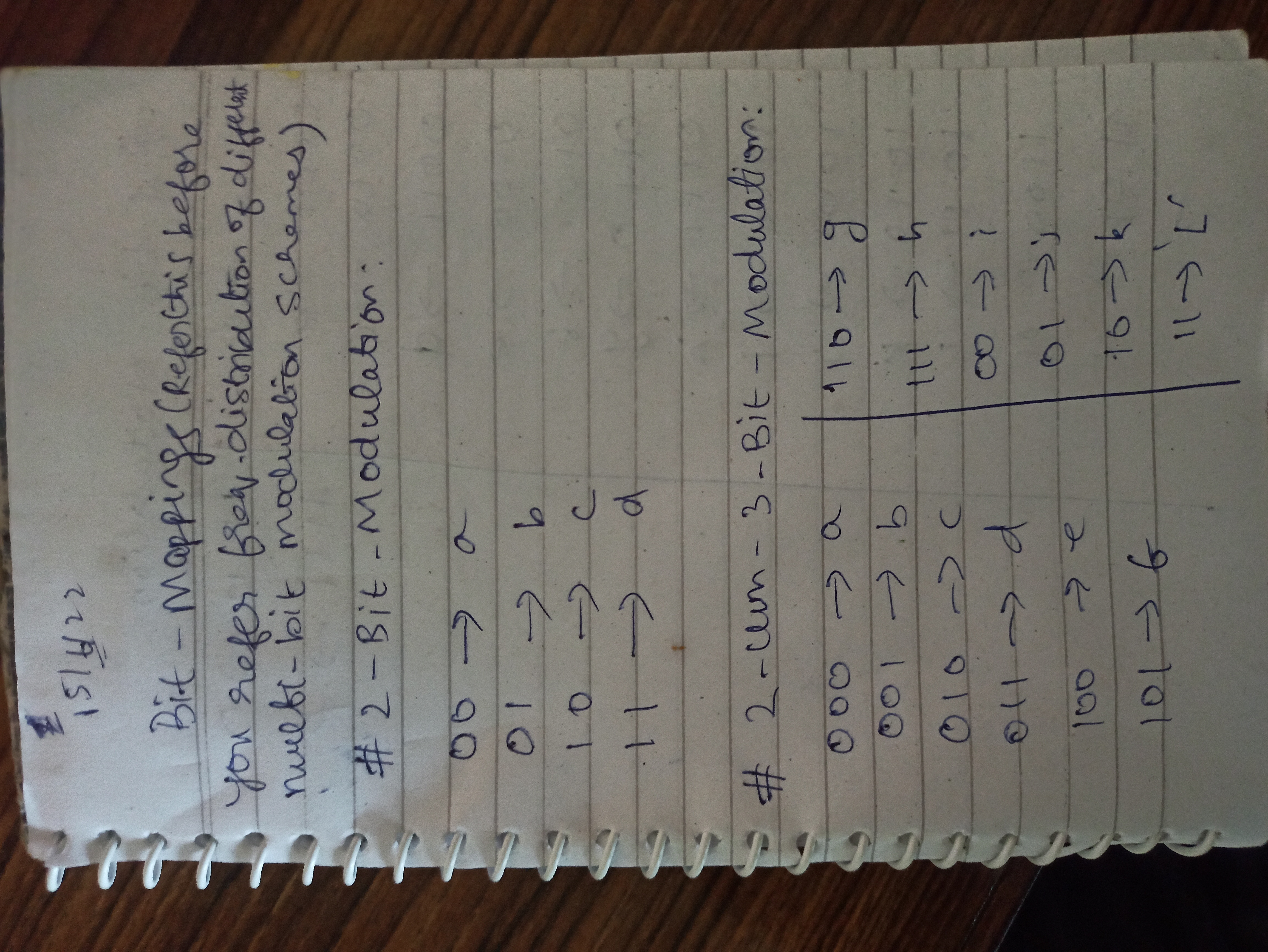
2 bit modulation!
2cum3bit modulation
and 4 bit modulation
I alloted symbols to each multi-bits and from (2 ms,18ms and on….upto number of levels).So one thing we can notice in the multi-bit-modulations are a tradeoff between number of pulsewidth levels with quantity of data, for eg, for 4 bit modulation there are 16 levels and the pulse width varies from (2 ms(1ms for on, one for off) to 256 ms!) but the number of data compresses to 96/4, for a 96 bit string. As per the freq distribution results i carried out the symbol allotment for different multi-bits and calculated the Theoretical data rate for 2 bit,2-cum-3 bit and 4 -bit are 95.6, 53.7 and 48.07 bps respectively. ,practical datarate might differ even starkly from this but this theoretical comparision ensures that even though the number of bits reduces for multi-bit modulation , the number of levels increase and the pulse width increases in steps of 17ms, essentially bringing down the bit rate , thus w bit theoretically has a good performance compared to 2 cum 3 and 4 , and 1 has a even good performance (100 bps for the “lot”) theoretically. (further research to be done on allocating symbols to each and every string individually as well as various other source coding methods). **Practically i used ST and got 64, 55.2 , 43 bps are their datarates and their BERs are 0.003,0.004 and 0.0074 in the mentioned order . Their Eb/No ‘s are 54,839 ,58,883 and 62,333. One thing is that even ST confirms the theoretical test that I had done above that multi-bit-modulations have lower datarate as you go on their line (in increasing no of bits per symbol fashion) **
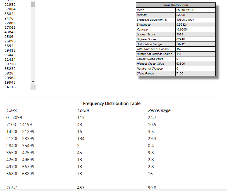
Find attached the stats that I used to calculate the metrics(ST) , for ####mod-using-android-studio-(17,43 ms prog delay for 0 and 1’s high time)
_statistics.png)
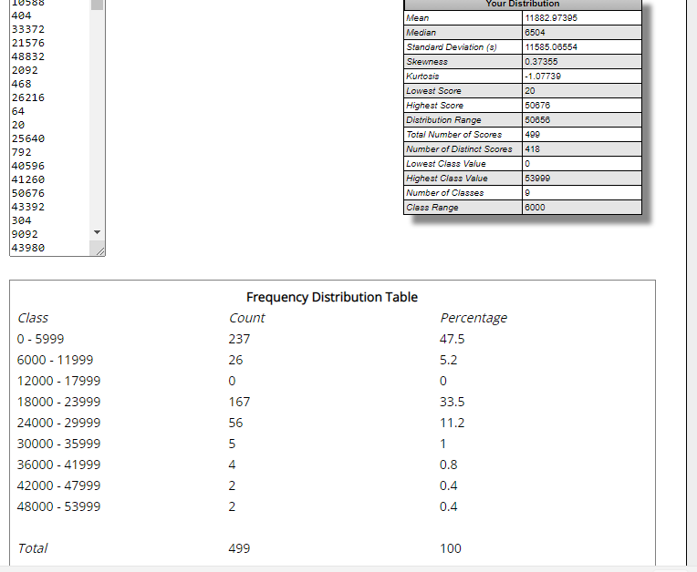
####mod-using-android-studio-(no-programmed-delay,17 ms prog delay for 0 and 1’s high time)
_statistics.png)
####2-bit-mod
####2-cum-3-bit-mod
####4-bit-mod
N. Finally i settled on the single bit modulation through android studio as the best hope until i came across several forums and answers from the queries that i posted which addressed “Rooting” the Phone and controlling LED driver through Shell maybe a better option. But Rooting is a dangerous process and a very unreliable one , which can brick your phone and erase all your data if not done correctly. I tried contacting several professionals in SP road, Bangalore for rooting my phone(the Electronics hub of Bangalore, possibly India) yet they refused citing it as potentially dangerous.
So i had to arrange for alternate mobile phones such as Lenovo K6 Power and Letv X509. I tried to root Lenovo and accidently bricked it as expected and rendering it useless. I succeeded in rooting the Letv but was unable to locate the exact flashlight driver and was unable to write any due to a denied permission set by SELinux. Came across Redmi and OnePlus phones being very developer friendly and thus i changed my personal phone to Redmi note 8 pro and used redmi note 5 pro as the goat for rooting, and eventually succeeded and was able to locate the flashlight driver.
O. Now to switch on and switch off i have to go to a file within the flashlight driver called brightness (an ascii file), i have to change the value of the file to switch the flashlight on at different intensity. Its values ranges from 0 (flashlight off) to 256 (the max permissible brightness, a limit set by the manufacturer , beyond which the flashlight will melt!) , This gives a possibility of amplitude modulation, but that’s an entirely different and there should be a dedicated effort towards it and my priority is different, I was able to switch on and off the flashlight by altering the file between two values 0 and 100.
P. Now , I needed to write a shell script to automate this, but unfortunately even though android is a linux kernel based system, its OS is different from typical Linux Distro, thus I came across the “Swiss Army Knife of Embedded Developers” in other words known as Busybox, which is a binary call which contains all unix functionalities packaged as a single unit. So I was able to use basic unix commands to interact with the android OS and I also downloaded Termux, which is a command line interface directed to android developers.
Q. Now with these tools I was able to write a shell script ( I was not able to use bash, since busybox just contains the essential utilities , was also not able to install due to the problem of SELinux, fortunately I was able to achieve my objective with the help of shell script in its own) , to periodically switch on and off the flashlight and with a delay (sleep function), and it maxed out at 400 Hz or 400 bps(average), which is much higher than my previous best 40 hz (for single bit mod through app). But without a delay I witnessed a magic, the frequency was a whopping 4000 Hz !!!!(average). Even though this method also has the same clock inconsistency problem, the average data rate here is very high because, essentially because when we consider the app developed through the android studio, it has to go through Camera Api and that camera API then finally controls the brightness file , whereas through shell, I was directly able to control the brightness file bypassing the camera API and saving me that delay.
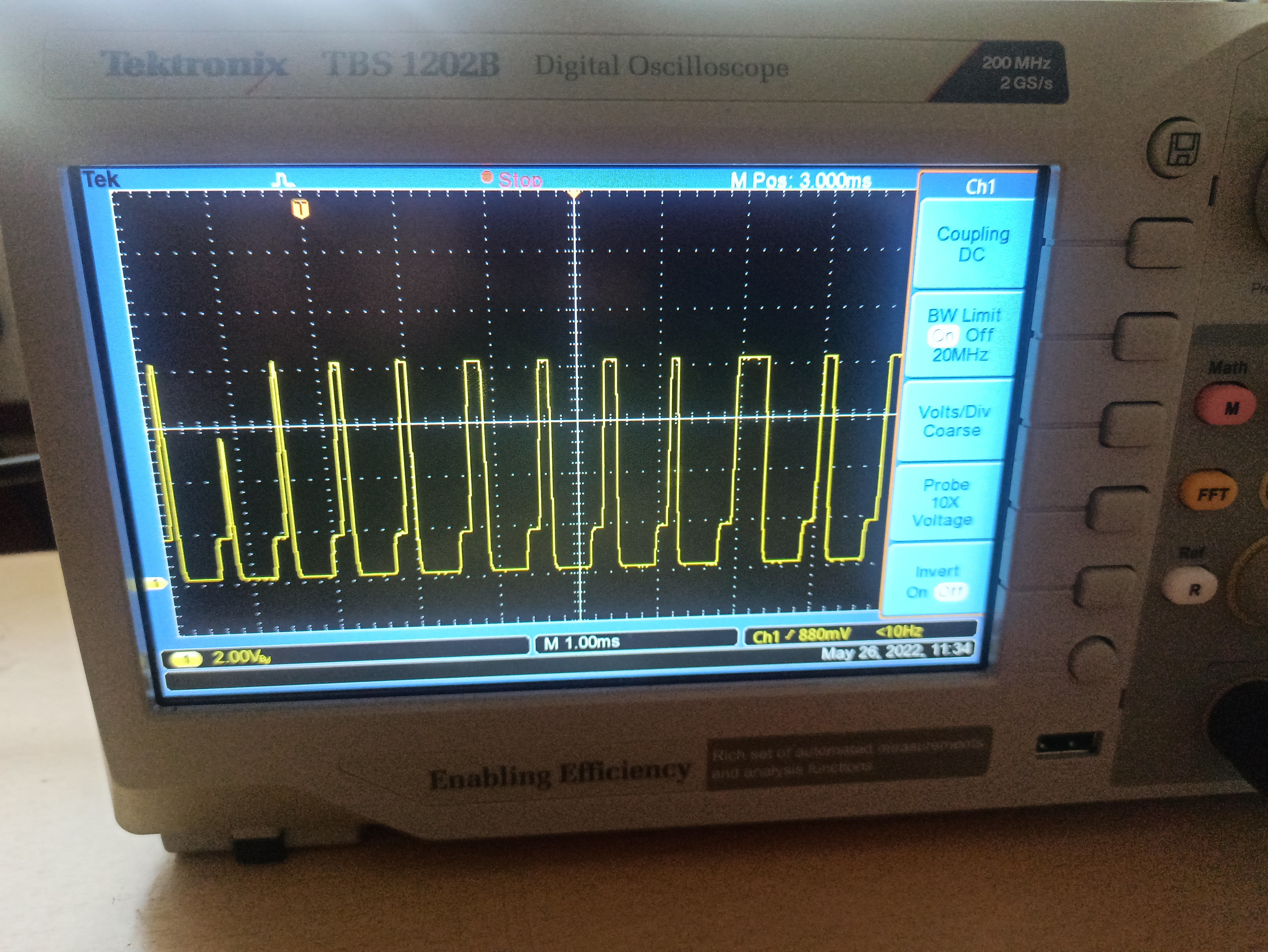
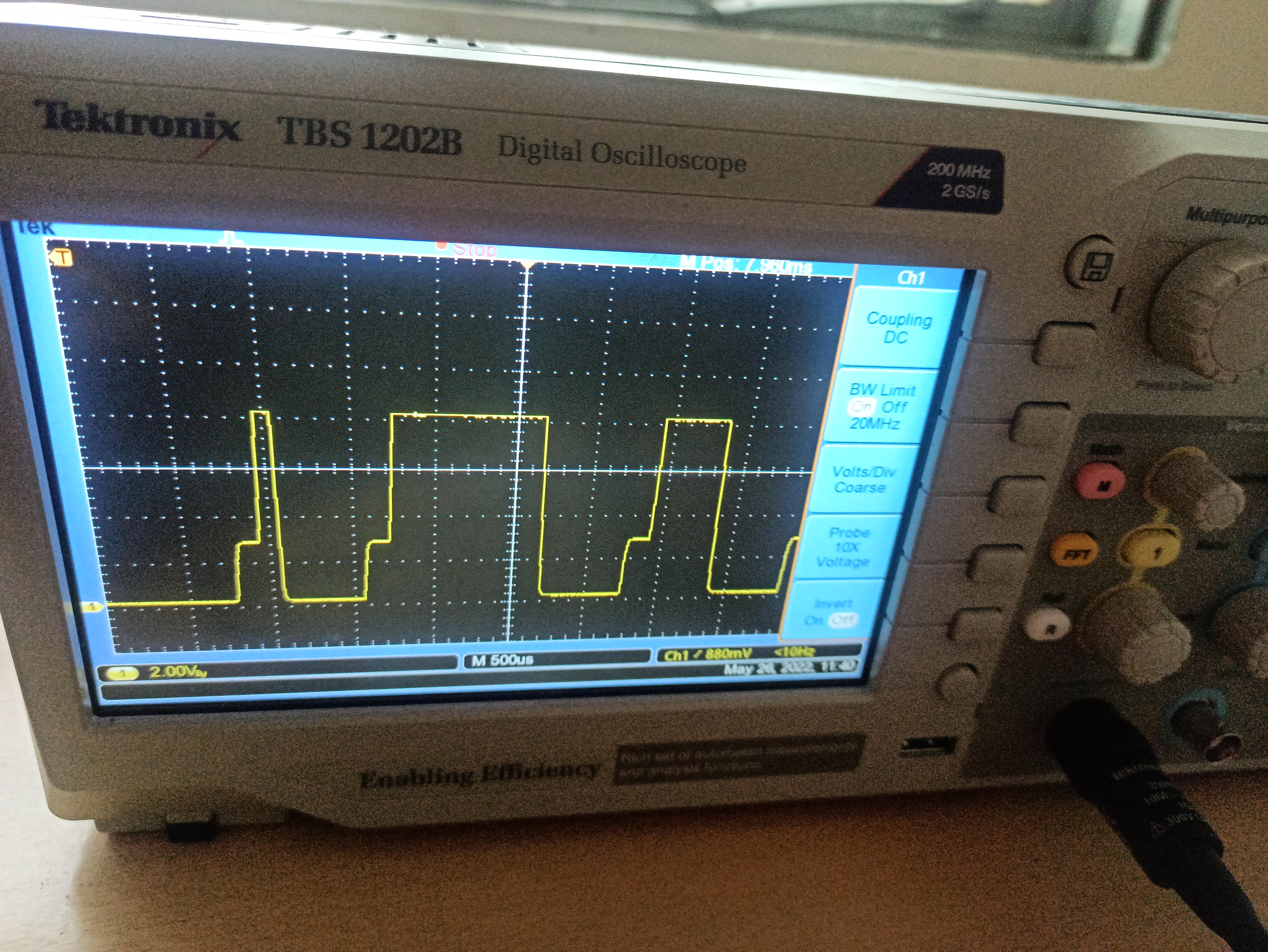
R. But subsequently my simple receiver ( bpw40- photodiode with arduino) was not able to receive the signal properly and it missed the pulses , primarily because both the photodiode and the reciever was slow( I used simple analogRead() rather than interrupts). As a solution I used a photodiode array designed and developed in IISc by my professor and a lm358 op-amp. Modified the receiver code completely using interrupts and was able to receive the signal correctly. This is the clock signal that i had obtained from my smartphone when programmed through shell with no delay
, want a zoomed version? here you go
Here is the stats
, we can see a 4000hz mean stuff here. Smartphone had a display failure and had to modify it but I optimized the total expenditure :D. Finally I tried transmitting data through shell (a 0 has a on and off with no delay , a 1 has a on with a sleep of 10 ms and off with 0 delay , but the average pulse width for high time was 19 ms
 , even lower than 15 ms of android studio’s latest mod that i have attached
which is done using android studio and has the camera api, despite that it outweighed this method , thus landing us to the statement that a sleep of 10 ms performs worse in shell compared to a sleep of 17ms in android studio and having a rate of 52 bps and BER as 0.0052 and Eb/No as 52,487 (ST) . But a delay of 5 ms in shell, ensures an average high pulse width of 10 ms, even though there is a 0.12% probability in average that your bit gets flipped for 1000 bits , but the datarate is nearly 100bps , BER and Eb/No is 0.0071 (ST) .
S.Thus Sleep is not very efficient in introducing delays at real time in shell, so I tried alternatives that can give me a precise delay
a. writing a cpp program and used chrono to introduce a delay and calling the cpp program from shell script, turned out to be slower than directly doing the same in shell. Also, using system() command in the cpp program , basically running shell script within cpp also similarly turned out to be slower.
b.Tried to use crontab and Hardware timers , but were not usable(crontab does not schedule jobs in micro or milli seconds).
c. Tried to introduce a delay using a for loop looping 100 times, and had a nearly consistent mean delay of 756 us though minimum and maximum delay drastically varied, thus using for loop is a good non-blocking way to achieve a delay at even lower scales compared to sleep function.
Ultimately, I came to know after reading several forums and querying several professionals who commented that a smartphone is a GPOS based device(General Purpose OS) whose design structure is very different from a RTOS(GPOS is like a internet system, it allocates resources to every activity without any discrimination rather than a RTOS which works on priority), thus one cannot expect guarantees out of a GPOS unlike a RTOS .
T. Now , run out of all methods, I perused for a while , if I reduce the pulse width difference that distinguishes between a 1 and 0 , there is a probability of 0 appearing as 1 and the probability of the inversion of bits increases , as I decrease the pulse width. Now then how can i differentiate a 0 from a 1 then seriously without increasing pulse width difference between them as well as not compromising on data rate , now obviously the possibility seems like I can only achieve one out of the two because this is no-brainer , because both of these things are contradictory! Well after deep thoughts,they are just seemingly contradictory , as there is a way! Surprising yet true! The difference is that when you stop thinking pulse width difference is the only Saviour! , and think of it as one of the saviors! , wanna know the other one, that’s voltage! Now you get caught when you only differentiate 1 and 0 based on pulse width, why don’t you also differentiate them based on voltage so that even if pulse width fails, voltage hails! :smiley: sorry for the punch! Now say , I add a 5 ms delay to 1 ’s symbol. Now the thing is the probability that 0 can pose as 1 is increased! But , I will add 0’s high time to be a lower intensity pulse and 1’s high time to be a higher intensity pulse. All the results and code related to this are attached in the results tab for your reference. I power the receiver circuit with 19 v source . The reason is for lower voltage powering , the flashlight intensity differences produces no voltage difference. Now 0’s high time has a 7.5 v value and 1’s high time has a 18 v value , Now my receiver checks if i receive a pulse it should satisfy 2 conditions to be a 1:
-It should have a delay >=5 ms -It should have a voltage greater > 10V.(the threshold is limited to the programmer , this is just a sample) .
Now for a 0 pulse, it has a risk of having high time pulse widths greater than 5 ms, but it gets caught at the second condition and rightly gets identified as 0 , provided condition 2. is always reliable!! And it is!
Thus , I should be able to rightfully classify 0s and 1s even though the pulse width data of both has an overlapping! I tried and kept the delay for 1’s symbol to 1 ms using sleep, and tried the modulation, it should be successful, as there should be 0 symbols whose pulse width might / will be (insight from past data ) greater than 1 ms, but they rightly will be eliminated to 0 as their voltage will be low (2.5v in my case, from 1 5v in my case) **but with one catch! The overall data rate is the same for my prev 5 ms delay case i.e 100 bps or Hz(ST). No matter how low I program the delay using sleep, 100 bps is the maximum I can carve out! (upon testing the program several times and calculating mean pulse width!) Because on average , no matter how low you program the delay using sleep the 1’s high time pulse has a delay of 20 ms!!! , this brings down my total data rate . I connected probed my output to oscilloscope and this is the output
_voltage_divider_op).jpg)
, there is a superb difference in voltage between 1 and 0 , but the data rate is still low! , look at the stats attached below**
But Loops to the rescue! As I said earlier for loop is a good non blocking way to introduce a delay unlike sleep and you can customize your delay to whatever value you need by appropriately running the loop some x no of times. But everything comes with a cost,1. introducing a delay at a particular value using loops are not that simple as using sleep 2. It does not offer you the absolute minimum guarantee that sleep function does. An example can be used to illustrate the above mentioned points! I can program a 1 ms delay using sleep very simply, just sleep(1) , but for looping, I determined that looping a for loop 500 times gives you the mean delay of 1 ms. The next thing is the minimum delay varied in micro seconds from 1097 us to 1200 us ( after repeating the looping for 10 times, mean delay of 1400 us). Thus it does not offer you a strong minimum delay guarantee like sleep ( no matter how long the delay goes, but sleep(1) can never be lesser than 1). But a smart kid should sufficiently decide the threshold, looping a for loop 500 times, the minimum delay never became lower than 1090 ms, thus one can decide 1000 ms as the safe threshold delay to separate 1 and 0 symbols, which is what I did! , I also repeated the experiment by running a for loop 100 to introduce a 750 us mean delay to 1 symbol . I should be able to successfully separate 1 and 0 , using VPWM( a name that I gave to the modulation that I thought out of my own head! Variable voltage cum pulse width modulation) , but I just tested the mean pulse width. The 1 ms delay one had a throughput of 1.01 khz or 1010 bps. At last! It has Joined the KHz elite club! , here’s the oscilloscope output and stats! without_voltage_divider
_without_voltage_divider_op).jpg)
stats
_stats.png)
, now I just need to write a receiver program to confirm the result by making it spit 1s and 0s according to the programmed voltage and pulse width! . But subsequently one morning I thought do I even need to introduce a delay? Because we don’t care if 0 and 1’s high time pulse width overlaps, we have voltage to the rescue! Then why do we care to introduce a delay? Ah! Simple thing we don’t need a delay , how? If we are using only voltage don’t we land at the very same problem we landed at the very first case , i.e clock inconsistency! ? Hmm, there is an obvious difference, if we don’t use any special symbol and if we simply denote 0 as a flashlight off and 1 as a flashlight on, we fail to synchronize the receiver , because it cannot interpret continuous 0s or 1s. But now iam using symbols for 0 and 1 which consist of both high and low, thus it can differentiate between continuous 1s or continuous 0s despite clock inconsistency ! That’s the thin line of difference! So a proper clock pulse in which a 0 is off and 1 is flashlight on cannot pass any relevant data due to clock inconsistency, but my smartphone had a 4000 hz mean clock pulse.
Now with my method in hand I should achieve 2 khz or 2000 bps data rate! I will spend 250 us( in transmitting off, on 250 off 250 totally 500) per bit extra compared to my clock pulse due to every bit having a symbol consisting of on and off! So I should be able to transmit data at about 50 ℅ of my clock pulse rate or capacity. This I programmed the smartphone accordingly to suit this modulation( I can call this on-off-voltage-modulation oovm yikes !😀). Now unfortunately , :sadface , the output was not as expected we expected! I tested it by programming a alternate sequence of 1s and 0s and probed the output to oscilloscope. Thus the output should be 5v square wave ,2.5v square wave ,5v,2.5v … and so on ( for 1,0,1,0… sequence) , but this is the output
.jpg)
Wonder why everything is same (in volts) ? Its because higher intensities flashes take time than lower intensity flashes thus they pose as lower intensity flash and move on ! This is an handicap innate to my smartphone flashlight system! Now, dejected I tried my next best thing! Delay for 1’s symbol using a for loop of 100 times, which introduces a mean delay of 750 us to 1’s high time. This clicks , not the photo but the output 😀
_without_voltage_divider_op).jpg)
with voltage divider ,
_voltage_divider_op).jpg)
and now iam able to flash at a mean 1.7k bps ,see the stats for yourself
Not that bad compared to 2khz! But I cannot pump to 2khz but can near 2khz by introducing appropriate delay(not for pulse width modulation! Remember we dropped encoding data with pulse width for the prospect of a better one! I just introduced the delay to give it some time to switch on to higher intensity flash). Now we can notice on the picture that I have attached, that for 0 it resembles a perfect square pulse, but for 1 it resembles a staircase (see everythin for urself at the forums link below) reason: same as above, innate to my smartphone, it flashes to a lesser intensity like 0’s high time level intensity and then goes on to flash at programmed higher intensity. I first made this mistake(post #60 , arduino forums) , (make it happen) fortunately I was able to achieve sampling voltage before falling edge and spit out the 0s and 1s. My BER is 0.00034 and Eb/No for 1 is 77459 and for 0 is 12,913 thus giving out an average of 45,196 (ST). (Note: all metrics have been calculated for 500 random strings as the message). Now this is a blockbuster achievement for smartphone based transmitters! This is the fastest I can transmit data in my smartphone! (I can go upto but not 2 khz, due to above mentioned reason) . Yikes! Target 👉👍👌 done and dusted, at least for now!
U. Got Feedback from several forum friends who advocated the use of NEC protocol and use of differential modulation. See the link below to find why i find them not suitable (https://forum.arduino.cc/t/is-there-any-arduino-module-that-can-do-my-job-when-interfaced-with-uno/998127/39) for NEC and (https://indianinstituteofscience-my.sharepoint.com/:w:/r/personal/vikramv_iisc_ac_in/_layouts/15/Doc.aspx?sourcedoc=%7BBD2ECAA4-7F0E-4515-A4E5-B29CA63A3D8E%7D&file=Document1.docx&wdOrigin=OFFICECOM-WEB.START.REC&ct=1657861348692&action=default&mobileredirect=true) for differential modulation.
V. {ONGOING} : Non-linearity in VLC transceiver circuits
NOTATIONS: [1]:ST( A test in which i flash 500 strings of the same word “chockalingam” , it is useful for deterimining BER and other metrics! for all the types of modulations, this is the standard test that i had carried out.)